Embedded antenna design mistakes
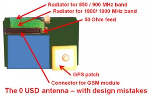
- Type: Meander with spiral
- Multiband (or GSM 900 / 1800 or GSM 850 / 1900)
- Not easy to tune on center frequency because the 900 MHz part goes straight to the 1800 MHz part
- Not easy to tune on antenna impedance
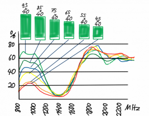
The GSM antenna structure at the picture is a shape that normally is in use with PCB antennas and coaxial cable. Such antenna structures are optimized on 4 to 8 cm distance to ground plane. A further design mistake is the ground area left and right of the antenna. Radio waves are travelling like light. The antenna is the “candlelight”. The ground area left and right will build shadows for the radio wave. The antenna structure is to close to ground plane and the connector is to close to the embedded antenna as well. Worst case the embedded GSM antenna will interfere with the GSM module. The GSM 900 part on the border of the PCB is very close to the plastic enclosure as well. The to close plstic enclosure will generate a parasitic load again. The blue marked area shows the “visible” ground plane of the antenna. Embedded GSM antennas like GSM chip antennas or embedded GSM PCB antennas are looking for 40 mm to 90 mm up to 40 mm to 110 mm ground plane. The blue aera has a size of estimated 40 mm x 30 mm.
Embedded GSM antenna on minimized ground plane
Read more: How will the ground plane effect your embedded antenna?
How to optimize this embedded GSM antenna design?
Start with reading here:
Nothing will interfere your embedded antenna?
And read all linked chapters!
GSM PCB antenna recommendations based on the picture
- Remove the embedded GSM antenna on small side of the PCB
- PCB size 40 / 50 mm x 90 to 110 mm
- Antenna needs bigger distance to ground plane
- No ground areas left and right of the antenna
- No parasitic load by plastic enclosure close to the antenna
- No parasitic load by the metal screws of the enclosure
- No cut and paste of an antenna structure
Not checked (details missed)
- Impedance of transmission line
- Number of PCB layers
- Number of vias
- Size of real ground plane area based on Gerber files
- Ground pins of GSM module to ground plane
- PCB tracks for supply voltage to GSM module
- Capacitors to block the GSM peak current
- Power supply to support the GSM module
- Place of the SIM card holder
- Capacitors close to SIM card holder
- Everything related to GPS
- Everything related to emission
- Everything related to radio approvals like R&TTE
This embedded design example has reach us, after finishing the first PCB. It is better to go the other way around. In the first step you tell the size and material of the enclosure. In second step a RF consulter will make a proposal for the antenna. The best and cheapest result you get, if you select the embedded antenna first and design the product around. Even better is, to give the freedom on a resonable size for a ground plane.
If you still not sure which antenna to select and why, then do not hesitate to drop an email to harald.naumann (at) gsm-modem.de

