GSM antenna designs mistakes in details
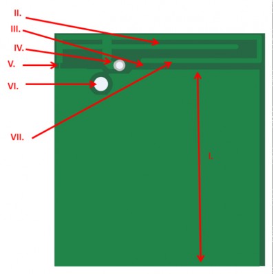
I. Size of antenna ground plane
If you compare the simulation of the GSM antenna in the IoT M2M Cookbook with
the antenna at the picture, then you will understand that the antenna efficiency at GSM 850/900 will be poor, because the PCB is already much to short. Nobody can cheat the physics. As soon the length of the PCB will less than 90 to 100 mm, the antenna efficiency at the lower band will shrink quickly.
II. Distance between the two GSM antenna radiators
The gap between the long radiator for GSM 850/900 and the short radiator GSM 1800/1900 is much too small. The small gap will reduce the bandwidth of the antenna.
III. Distance between the GSM antenna radiator for 850/900 MHz band
The gap is much too small as well. As bigger the gap is as bigger is the bandwidth of the antenna. You can compare the gap at the picture to the simulation in the IoT M2M Cookbook and will understand that the selected distance is completely wrong.
IV. Via hole in the antenna feeding
The via will add you a capacitor and an inductor in the antenna feeding line. The value of the capacitor and an inductor is related to the size of the whole and the thickness of the PCB plus Epsilon R of the PCB. If possible, then do not have a via in the feeding line of the antenna. The PCB has at least two layers. If you just put the antenna structure on the other side of the PCB, then the problem is solved.
V. Width of PCB structure
The width of the antenna structure will interfere the bandwidth of the GSM antenna as well. The width of the whole antenna structure is already too small in comparison to the antenna in the IoT M2M cookbook. On top of the too small PCB tracks, the shorting point of the antenna has a tiny PCB track to ground.
VI. Big via hole close to the GSM antenna
Each IFA or PIFA has a need for a big homogeny ground plane. The ground layers of the top layer and bottom layer or inner layers can be connected together to a ground plane. The distance of the vias is related to the highest frequency you plan to transceive. Anyhow, big via hole close to the border of the ground layer will not allow that the RF currents will flow unimpeded. The rest of the shadowed PCB was full with holes for trough hole connectors as well. The whole PCB looks more like a “Swiss cheese”, than a homogeny ground plane.
VII. Bending of the antenna radiator for the lower GSM band
In the IoT M2M Cookbook was told “Do not bend” and in this layout the PCB track is already close to a snake structure.
Analyse of GSM PIFA antenna summary
I have seen the same antenna structure in another design before. It did contain all mayor mistakes like usual. I assume it is a copy of a copy of a copy without to understand the basics of antenna designs. It is possible to design an own PCB antenna integrated in a PCB to save costs, but without to have the details and just by cut and paste you will run in trouble. If you plan to develop your own PCB antenna shape and have no know how or no network analyser, then it is better to select a third party.
The best and cheapest result you get, if you select the embedded antenna first and design the product around. Even better is, to give the freedom on a reasonable size for a ground plane.
If you still not sure which antenna to select and why, then do not hesitate to drop an email to harald.naumann (at) gsm-modem.de
