Calibration of the VNA on PCB with embedded antenna

Calibration of the VNA on PCB with embedded antenna
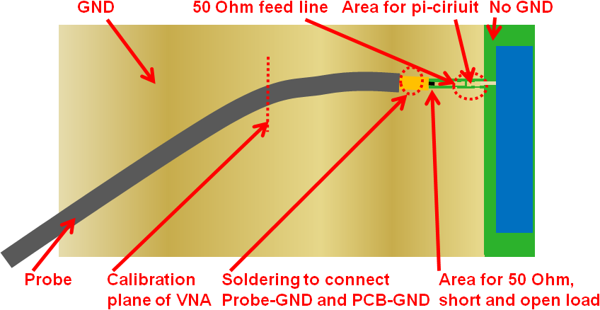
The calibration of the VNA (Vector Network Analyser) for a PCB with embedded antenna is difficult. The final antenna with all components except the wireless module should be mounted inside the final enclosure. The wireless module will be replaced by the probe. The three calibrations of the VNA for short, open and load will be done directly on the PCB. The probe will be a top quality coaxial cable directly soldered to your PCB. The short load, open load and 50 Ohm load have to be close together on the same plane. The first step is to mount the probe onto the PCB. Replace the isolation of the probe cable (orange area in the picture) and solder it onto the PCB. Be careful that the inner conductor of your coaxial cable is not too long because this could force a shift in the calibration plane. You will achieve the short load by soldering the inner conductor to ground and the 50 Ohm load by soldering a 50 Ohm resistor to ground of your PCB. Please use a small 50 Ohm resistor of a type of 0603 or even smaller. Please note that two 100 Ohm resistors in parallel will decrease the parasitic inductance of the resistors and the result will be a more accurate calibration. If you have a small PCB with a small antenna you can’t use a thick coaxial cable (e.g RG174 or RG213) and a large coaxial connector. Not only is this impractical – how to connect the connector type SMA or N – the metal bulk will also affect the antenna and grounding properties of your PCB. The measurement will be useless.
We recommend the use of the small and popular U.FL connector and its associated cables. The U.FL socket fits on almost any PCB and it can be improvised on your printed circuit board without a U.FL footprint. With the U.FL calibration kit, you can match several PCB layer stacks. The OPEN, LOAD and SHORT on the U.FL calibration kit is done three times. The mass layer is on the button layer, layer 1 or a layer in the middle of the PCB. The calibration will be done on the layer stack which is closest to the PCB with the embedded antenna. It is recommended to place a U.FL connector on your PCB during development. However, in the worst case, the U.FL connector will be placed by scratching the solder resist and cutting the 50 Ohm micro-strip line.
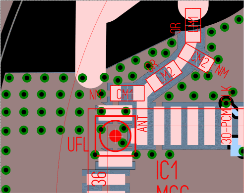
The picture on the left is out of a real IoT project with a GSM module. The non-visible PCB antenna is a modified GSM inverted F antenna public in the previous chapter of this IoT / M2M Cookbook. You will detect a lot of vias close to shorting the interfered F antenna. The GSM module is very close to the antenna and the main PCB is small as well to save board space. The whole PCB including the self-made PCB-antenna has a diameter of only 70 mm. If you drive the PCB board space to the limit then you have to spend much more effort, time and money, but for this € 100K+ IoT project, it was justified. The second picture was made by moving the module on the PCB out of the way by a few mouse clicks to show the common assembly of a U.FL connector.
If you have PCB space left, then it makes sense to place three U.FL connectors: OPEN, LOAD and SHORT close to the U.FL connector. As described earlier you can achieve the LOAD with two 100 Ohm resistors in parallel or even better three 150 Ohm resistors in parallel placed in a star configuration This will increase the upper-frequency limit of the LOAD calibration. It is recommended to use 2 x 100 Ohm or 3 x 150 Ohm type 0402 resistors in parallel. It is a little bit difficult to solder, but in this way you decrease the parasitic inductance of the resistors. Please mount the resistors upside down to further help decrease the parasitic inductance. The carbon layer in the resistor should be mounted to be considered as a small length of a 50 Ohm line. If possible then do not reuse the same 50 Ohm micro-strip line by soldering and de-soldering the resistors. Use as low as possible solder alloy and take care to perform excellent soldering. For the SHORT you can use plain tin-solder instead of a 0 Ohm resistor. If you use a 0 Ohm resistor then mounting it upside down will help to control parasitic inductance as well. The higher the frequency range, the more important is it to take care of parasitic inductance and to achieve accurate soldering.

U.FL connector parallels to the radio module
For this PCB the U.FL connector was placed to the left side of the antenna pin. This was only possible because the antenna pin was at the corner of the wireless module.

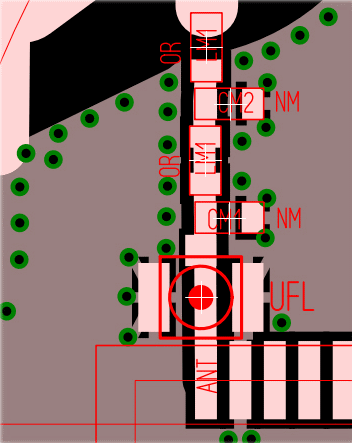
U.FL connector in row to 50 Ohm micro-stip line
For this PCB the U.FL connector is in front of the antenna pin of the wireless module. This is the common approach for modules where the antenna pin is not at one corner.
After the calibration, save the calibration file with a meaningful name on your hard disk. If you have already performed the calibration with a SMA calibration kit as described in the earlier chapter, then this will be the second calibration file on your hard disk. Further files will certainly follow and so it is important to use meaningful file names to help you organise the readings to separate projects. The next steps are the same as for the four antennas described in the last chapter. You will measure the antenna without a matching circuit and load the S1P files to Atyune. With Atyune you will calculate the capacitors and inductors for your antenna project, and as a further step you solder the calculated components to your PCB and repeat the measurement. The result will be a matched antenna. If you already have the soldering pads of the inductors and capacitors in your layout, then you need to close the gap for the component in series to your 50 Ohm feeding line with a 0 Ohm resistor. An additional option will be to produce the prototype PCB without a gap, to measure the PCB with the antenna and then to scratch a solder pad using a scalpel.
There may be, however, some more steps required. If you detect that the resonances of your PCB track GSM antenna are too high, then use a scalpel and start by scratching the radiators. By shorting the length of the radiators the resonant frequency will rise. If the resonating frequency is too low, then this is the worst case and just bad luck. You may need a new PCB. If you have time to play with the impedance of your antenna, then just produce some different antennas by shifting the shorting link several times. The result will be a shifting of the impedance and a shifting of the resonant frequency as well. If the power consumption of your application is important, then good matching will be important to decrease the TX power. The better the matching of the antenna, the lower the power consumption of your IoT / M2M device will be.
Such a prepared PCB can be measured on Return Loss and matched for estimated USD 500 to USD 1000. If you are interested in antenna matching, then do not hesitate to drop an email to harald.naumann (at) gsm-modem.de .
I did a shoot-out between AnTune, Betamatch and Atyune. AnTune was the fastest and solved the matching circuit equations with results that I was able to solder (0402) and prove experimentally. Betamatch was more flexible (cartesian graphs for BWP for example) and also gave accurate results but wasn’t as fast. Atyune was a bit slower but came up with matching solutions which, when implemented, were not always accurate.
AnTune is my chosen solution. It works well with LAN connected Agilents and also Copper Mountain Technologies instruments (USB).
I prefer Atyune in combination with the VNA of http://www.megiq.com. MegiQ is cheaper then Agilents and also Copper Mountain Technologies instruments and more handy as well
Hello, do you place the 50ohm load close to the connector or to the antenna ? Thank you !
It depends on the application. Most time the wireless module is close the antenna to avoid interference with the 50 Ohm microstrip line. The load for the VNA is often at one of the places for components in the matching circuit. Furthermore, we use a separate calibration PCB to avoid to solder Load, Short and Open in the final PCB.
I tried to optimise an 868 MHz PCB print Antenne with this method. Because the application board including the antenna was less than Lambda/4 of wavelength, i had a big influence of ground extension bei the semi regid coax cable metal shielding. How can I reduce this influence of the measurement cable ? You metioned some kind of ferrit beats across the measurement cable ! Could you please give us an example of this beats ? What kind of beats did you us ?
The distributor of your VNA should be able to help with the ferrit beats.