Bluetooth, WIFI, ZigBee, ANT, and Wireless Hart – all mentioned radio protocols are using the 2400 MHz band
Even the GNSS band (GPS, Glonass, Galileo, Beidou, QZSS) have to follow the same specifications, because 1575 MHz to 1610 MHz is not far away from the 2400 MHz band. Chip antennas and PCB antennas can be used for GNSS as well. The only what you will miss by using chip and PCB antennas in GNSS applications is the circular polarization. The circular polarisation you get with GNSS patch antennas or helical antennas mainly. In handheld devices is often no space left for an antenna with polarisation. If you open a smart phone, then you will not find a GNSS patch antenna. Even chip antennas are rare to save costs. You will find a bended piece of metal or just a slot in the metal frame.
The chip antennas for GNSS and the 2400 MHz band we can divide in monopoles that has one input for feeding the antennas and loop/PIFA that has a feeding pin and another pin to ground. The PCB track antennas we can divide in monopole and inverted F antenna. There are further options to build a small antenna, but those are not part of this paragraph.
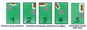
Ceramic loop/PIFA antenna (picture 1)
The ceramic loop/PIFA has a connection on two sides of the antenna. One pin is connected to the transmission line. The other pin is connected to ground. These ceramic chip antennas are often symmetric. It does not matter in which direction it will be mounted on the PCB. Such antennas have regularly a gap with non metal between the antenna and ground plane (on ground chip antennas are rare). This non metal area means non metal on all layers of the PCB. If you have a multi layer PCB, then it makes sense to design the gap on the inner layers a little bit wider. The bottom and the top layer will be used for tuning. The gap can be adjusted by scratching cupper on the bottom and top layer during tuning. With the matching circuit it is possible to tune the antenna as well. If you have a closer look at the data sheet and guide line of the embedded GPS chip antenna, then you will find a length of the reference PCB of 80 mm. The chip antenna is exact in the middle of the 80 mm. If you reduce the 80 mm to 46 mm then you will lose antenna efficiency. The 40 mm to 23 mm left and right of the antenna has to be symmetric. For 2400 MHz applications the standard length is smaller, because the resonant frequency is higher. Please note that you can expect the antenna performance listed in the data sheet only if your design will be close to the reference design. Everything else is a compromise with losing a part of the antenna performance.
Ceramic monopole antenna (picture 2 to 4)
Ceramic monopole antenna you will find at the edges of the PCB. This type of antennas has it need for free space as well. The free space has to be on all PCB layers too. By having a closer look on the dimensions of the antenna in 3D and on the bandwidth you will see that the bigger antennas offer a bigger bandwidth and better performance as well. As bigger the bandwidth is as easier it is to fit in the necessary bandwidth in. At GNSS it the bandwidth is already small, but GNSS is not just GPS anymore. GPS is on 1575.42 MHz and Glonass is up to 1610 MHz. Right now a lot of embedded GNSS antennas cover GPS only. This will change for sure. All new smart phones cover GPS and Glonass. If your device will not support Glonass then the Russian government will charge 25% tax. Combined devices will be taxed with 5% only. Glonass only devices will be not taxed extra.
Back to size and bandwidth: If size does not matter, then select the bigger ceramic antenna. Compare not just the dimensions of the antenna. Have a look on the necessary free space as well. The real space for the embedded antenna is the dimensions of the antenna in 3D plus its free space in 3D.
Ceramic monopole antenna with stub (picture 5)
Most ceramic monopole antennas can be optimized / tuned with a short PCB track on the end of the antenna. Just take care on some free space for the stub on the open end the antenna. With a small PCB track you will the antenna structure a little bit longer. As longer the antenna is, as lower will be the resonant frequency. With such a stub you can reduce the resonant frequency only. If you would like to increase the resonant frequency, then just select another chip antenna from same vendor out of the same antenna family. Be aware that the distance to ground is an option to tune the antenna as well.
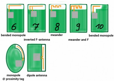
PCB monopole antenna – bended monopole (picture 6 and 10)
If you design the PCB monopole antenna at picture 10 right then you get a nearly omnidirectional radiation with loosing of 3 dB antenna efficiency. Sometimes it is better to accept 3 dB loss and to reach an omnidirectional character of the antenna.
PCB inverted F antenna IFA (picture 7 and 9)
If you do not make just a one to one copy, then the inverted F antenna gives you some more options than an embedded monopole. The mentioned rules on distance to ground and free space are related to the IFA as well. There are tons of inverted F antenna shapes listed on Internet. Most of them are copies only and a lot of them are copies of copies. Remember, that even the PCB thickness will effect on the antenna parameters as well.
PCB meandered antenna (picture 8 and 9)
PCB meandered antenna will reduce the mechanical width of the PCB. Meandering of a PCB structure always means a reducing of the bandwidth. As told before any antenna you will select is a compromise often.
Monopole antenna at proximity tag
It is just an example for a bended monopole antenna in a round shape. Be aware that the radius of the antenna shape will affect the antenna performance as well.
Dipole antenna
Dipole antennas are rare in small designs. The reference designs for radio modules / ICs are most time based on monopole antennas. GNSS modules and a lot of other RF modules offer a non symmetric 50 Ohm output to ground. To catch the benefit of dipole antennas you have to invest in a customization.
If you still do not know which antenna type to select for your application, then do not hesitate to drop an email to harald.naumann (at) gsm-modem.de
-
Nothing will interfere your embedded antenna?
-
Why the embedded chip or patch antennas are resonant on the wrong – to high – frequency?
-
How will the ground plane effect your embedded antenna?
-
Which radio approvals has your M2M device to pass?
-
How to connect your embedded antenna with your wireless module?
-
How to design an antenna matching circuit?
-
How to switch between an internal and external cellular or GNSS antenna cheap?
-
Which GPS antenna shall be used for a tracking device?
-
Which embedded antenna to select for a Bluetooth / GNSS application?
-
Dos and don’ts during embedded antenna design in
-
Examples for good and bad M2M designs with embedded antennas
- Q&A: Design in of embedded antennas


Dear Harald,
Excellent!!!
Kind regards,
Claudio
very very instrasting information .
Can I get pension of monopole bended PCB antenna
Please provide dimension of monopole PCB antenna
Sorry, but I do not understand your message.
Hi Vallinath, but you can not copy an antenna layout to your PCB without to test it by your VNA.